 한국어



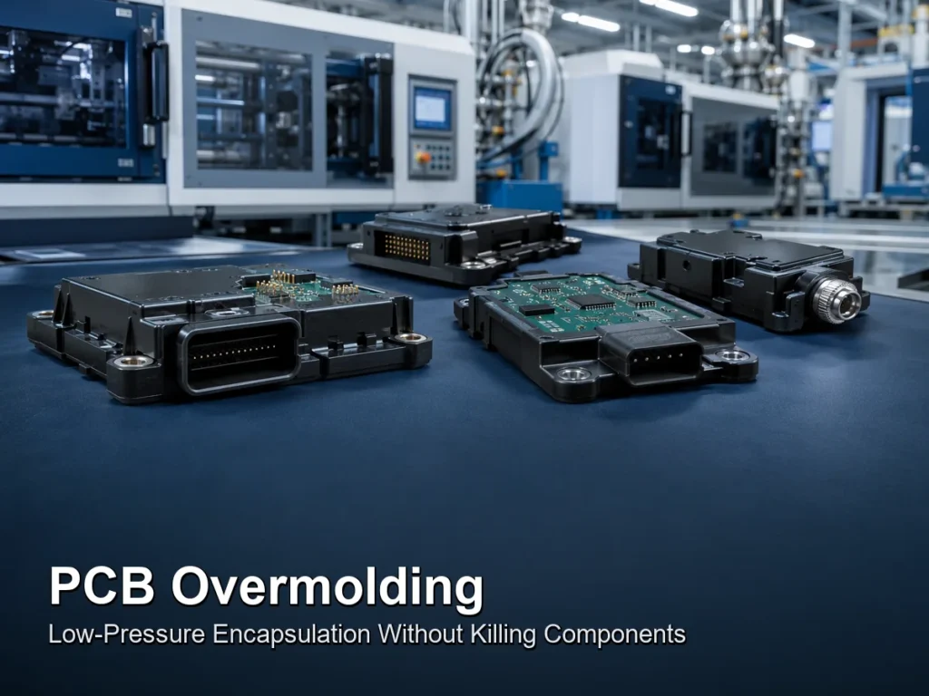
TL;DR, the honest version: PCB overmolding is not injection molding with a circuit board in it. It is a contest between two numbers — the pressure your melt needs to fill around capacitors and connectors, and the pressure your solder joints and brittle components can survive before they move, crack, or open. Everything else in this guide is downstream of that arithmetic. Most published guides stop at “use low pressure and inspect carefully.” This one works the force calculation through, separates the three genuinely different processes that all get sold as PCB overmolding, and gives you the reliability evidence that should exist before you accept a production lot.
A customer brought us a batch of overmolded control boards that passed cosmetic inspection and failed at the customer’s line: continuity open on one net, ten percent of boards. The moulding was flawless. A 12 mm tall connector had shifted 0.3 mm under second-shot flow because nothing in the tool located it — the board alone was the datum, and the board can flex.
Key Takeaways
- Three different processes share one name. High-pressure thermoplastic overmolding, low-pressure hot-melt encapsulation, and potting are not variants of each other. Choosing the wrong one destroys the assembly, quietly.
- The design load case is force on components, not fill. Cavity pressure multiplied by the projected area of a component face is a real number in newtons. Solder joints and brittle bodies have a limit. Compute both before you pick a process.
- Locate the board on hardened features, not on components. If the tool’s datum is a connector or a board edge that can flex, the board is a fixture, not a part.
- Moisture is the silent defect. A hygroscopic encapsulant moulded over a board that absorbed humidity during storage turns your cooling phase into a steam generator.
- Verification is electrical after moulding, not before. Whatever passed reflow test is not what shipped; dielectric, continuity and thermal cycling belong downstream of the tool.
Why Trust This PCB Overmolding Guide?
Ideal Pro designs the tool, runs the moulding and owns the dimensional and functional inspection under one ISO 9001:2015 system in Huzhou, on presses up to 1,600 tons, with over a thousand mould sets built a year. We are candid about the boundary: we do not run IATF 16949 or an implant-class medical device path, so boards destined for automotive safety functions or regulated medical should go to suppliers who live inside those audit systems. What we can do is tell you where the component-force limit sits, what the tool must locate on, and which artefacts should exist before a production lot ships.
Numbers below are either our published shop standards, arithmetic on stated assumptions, or process windows to argue with your machine supplier — labelled each time. Where a figure depends on your component layout, your laminate, or your reflow profile, we say it depends instead of inventing a universal number that would read better and cost you more.
Quick Reference Guide: Which “PCB Overmolding” Do You Actually Need?
This table settles the argument before the quote. The three processes differ by two orders of magnitude in fill pressure, and the board only tolerates one of them.
| 프로세스 | Typical fill-pressure scale | Material family | Use it for | Kill it when |
|---|---|---|---|---|
| Conventional high-pressure overmolding | Tens of MPa at the cavity | PC, PC/ABS, ABS, PA, PBT | Boards with only rugged, well-anchored parts; structural housings moulded around a bare or lightly loaded board | Tall brittle components, BGAs, large connectors, fine-pitch parts |
| Low-pressure thermoplastic encapsulation | Low single-digit MPa — confirm with the machine maker | Hot-melt polyamide, TPU and specialty low-pressure grades | Populated PCBAs needing insulation, moisture and vibration protection without potting’s mess | Long-term high-temperature service, aggressive solvents, thin flow paths |
| Potting / encapsulation | Near-zero — it is poured, not injected | Silicone, polyurethane, epoxy | Irregular geometry, heavy connectors, maximum environmental protection, low volume | Cycle time matters, weight matters, you need a clean edge for a mating part |
Our overmolding capability page states plainly which of these we run in thermoplastic; if a drawing lands in the third row, the right answer is to tell you to buy a potting line, not to pretend a moulding tool will do it.
What Is PCB Overmolding?
PCB overmolding is the injection moulding of a polymer directly onto a populated printed circuit board assembly so that components become permanently embedded in an insulating, sealed shell, with connectors and terminals left exposed through the moulded surface. The defining constraint is that the object being moulded around is an electrical circuit with mechanical joints — solder — that were engineered for a completely different load case than the one you are about to apply.
Why anyone does it: it replaces a housing, a gasket, a conformal coat and an assembly step with one operation. You get dielectric isolation, an environmental barrier against humidity, wash-down and vibration, strain relief at the connector, and a body you can mould ribs, snap-fits and branding into. What you give up is serviceability, and that trade is usually permanent: you cannot un-mould a board. Whatever is inside that shell has to be right before the tool closes, which is why the inspection step sits where it does in the sequence.
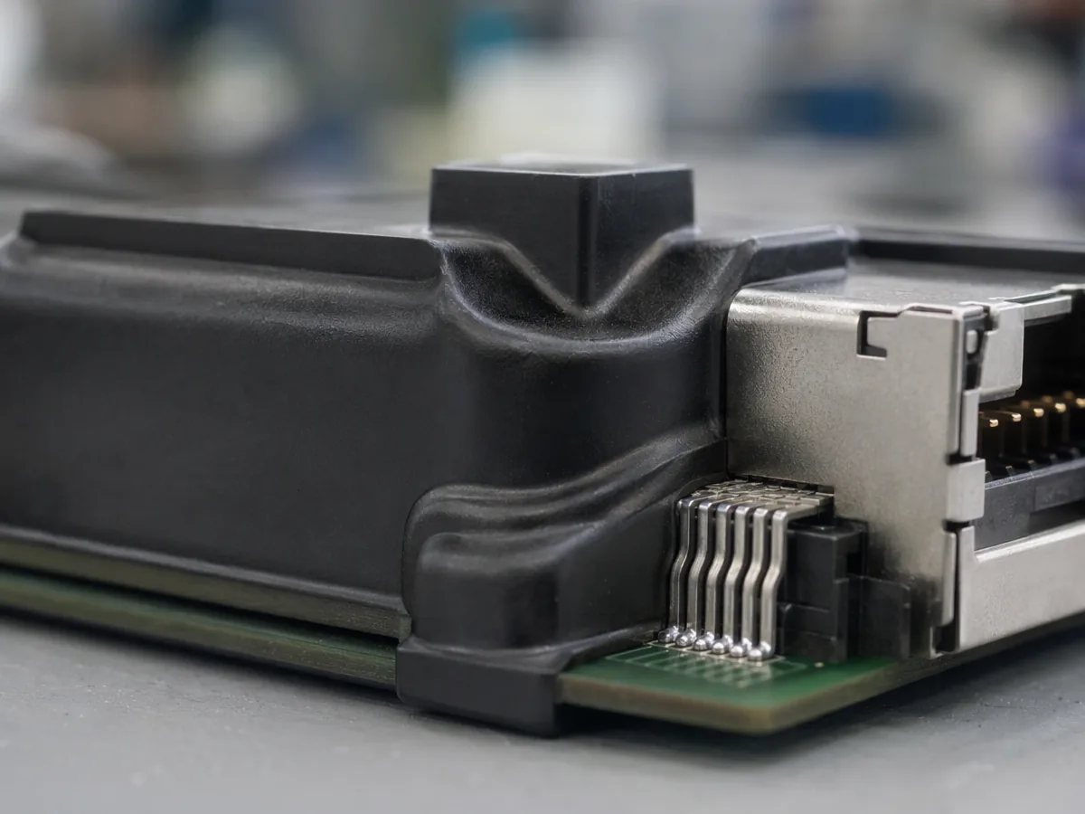 Figure 1: The interface that matters. Polymer meeting a connector body is where seal integrity and field returns are both decided.
Why Can’t You Just Use Standard Injection Molding on a Board?
Because cavity pressure multiplied by component projected area produces a force that solder and ceramic bodies were never designed to carry. Melt does not know your board is a circuit. It applies pressure to every face it touches, and it applies it while the solder is in a freshly reflowed, thermally stressed condition.
Here is the arithmetic you should actually run, on your own geometry, before you let anyone quote a tool:
- Take the residual or peak cavity pressure the process will impose. Conventional molding is tens of MPa; low-pressure systems are commonly quoted in the low single-digit MPa range — a difference of an order of magnitude or more, and the exact reason the second row of the first table exists.
- Multiply by the projected area of the tallest, most poorly anchored component facing the flow. A 2 mm × 2 mm face is 4 mm², so a nominal 1 MPa of pressure is roughly 4 N on that part; the same face at 30 MPa is around 120 N.
- Ask what the joint can take. A solder fillet’s resistance depends on wetting, pad geometry, component mass and the direction of load, and it is not published on your BOM. This is the number your EMS partner has to supply, and it is the number that decides the process.
- Do it again for the connector. Connector bodies are large, tall, and frequently retained only by solder and a small plastic latch — the highest-force, lowest-anchored object on most boards.
The second constraint is heat. Engineering thermoplastics need melt temperatures that push against what a populated board tolerates: existing solder must not reflow in a way that shifts parts, and laminate, adhesives and electrolytic components have their own ceilings. This is a genuine conflict, and it is why the low-pressure branch of the process exists at all rather than being a marketing invention.
The third is warp. A board is thin and stiff in one direction only. Pressure on one face bends it, the tool holds it bent, polymer solidifies, and the clamp releases. Now your board is curved and your connector coplanarity is a memory. Board-support features and balanced fill are not refinements; they are how you keep the part flat.
“Every PCB overmolding problem I have been asked to rescue was a fixture problem disguised as a materials problem. The polymer behaved exactly as designed. Nothing was holding the board.” — Ideal Pro moulding process lead.
What Must the Tool Locate On?
A PCB overmolding tool needs a datum that is harder than the part and immune to melt pressure. In practice that means machined support pads under the laminate, dedicated locators around hardened features, and a rule nobody should be allowed to break: never locate against a component.
- Board support under the laminate. Land support on bare FR-4 zones, distributed so the unsupported span under any component is short. Support directly under a large BGA or a tall capacitor concentrates load exactly where you cannot afford it.
- Connector fixturing. Locators that capture the connector body itself — moulded bosses or machined pockets — because the connector is the feature that must stay coplanar with the board and out of the flash.
- Clip and shut-off clearance. Melt will find every gap around a board edge and produce flash measured in tenths of a millimetre. Tight shut-offs around the laminate, and a plan for the flash you accept anyway.
- Automation features. For volume, moulded locator bosses or an added carrier let a robot load repeatably. Hand loading is a per-part cost and a per-part variable that never stops being a variable.
- Vent at the end of flow, and where air gets trapped by tall parts. Trapped air around a tall connector gives you a short or a burn in the same place every cycle.
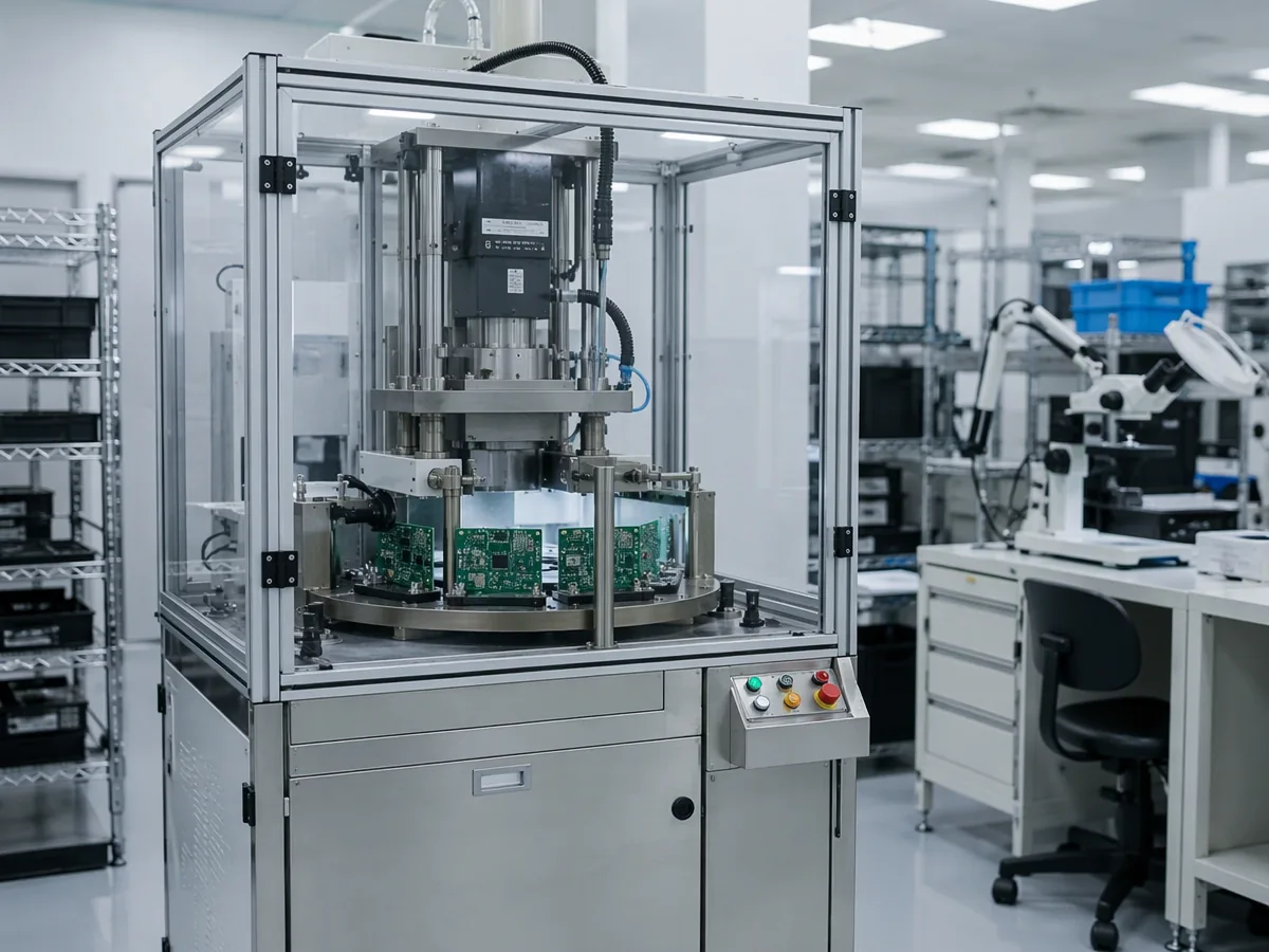 Figure 2: A low-pressure encapsulation cell. The machine’s defining spec is not tonnage — it is how gently it can fill.
Which Materials Suit PCB Overmolding?
Encapsulant selection is a ranking of four competing properties: how gently it can be processed, how well it blocks moisture, how much heat it must survive, and how it behaves across thermal cycling against FR-4. No material wins all four, and the coefficient of thermal expansion mismatch with the laminate is the property that shows up years later.
| 재료 | Processing | Strengths | Limits you will hit |
|---|---|---|---|
| Low-pressure polyamide hot melt | Low pressure, fast set | Good moisture resistance, quick cycles, flexible grades available | Narrow service-temperature window; verify compatibility with your conformal coat and adhesives |
| TPU | Low to moderate pressure | Tough, abrasion resistant, good strain relief at cable exits | Hygroscopic — must be dried; upper temperature ceiling |
| 폴리우레탄 | Mostly potting | Flexible, excellent environmental barrier | Cure chemistry to control; exotherm on mass; long cycle |
| Epoxy | Potting | Highest chemical and mechanical resistance, rigid | Brittle under cycling, exotherm can cook parts, effectively un-repairable |
| 실리콘 | Potting or LSR moulding | Widest temperature range, very low stress on parts | Lower mechanical strength; adhesion needs primer; contamination risk for later bonding or painting |
| PA / glass-filled PA | Conventional high pressure | Structural bosses and snap-fits moulded to the board | Only where parts are rugged and anchored; very hygroscopic |
Drying is not optional for the polar families. Our resin drying guide covers the dew-point and dwell discipline; applied to boards it matters twice, because you are drying the encapsulant 그리고 the laminate has its own moisture budget. A board that sat open in a shop for a week can release enough vapour at melt temperature to leave voids at the interface — the kind that pass visual and fail a thermal-cycle qualification.
Where the part needs a structural grade rather than a soft one, check the material pages: nylon, TPU, 및 TPE. If you want the wider bonding theory behind all of this, read the plastic overmolding guide first.
What Does the Flow Front Do Around Components?
Melt arriving at a populated board does not flow through a channel; it flows around obstacles, splits, re-welds, and leaves cold joints wherever two fronts meet past a tall part. Those weld lines are simultaneously your mechanical weak points and your air-trap locations.
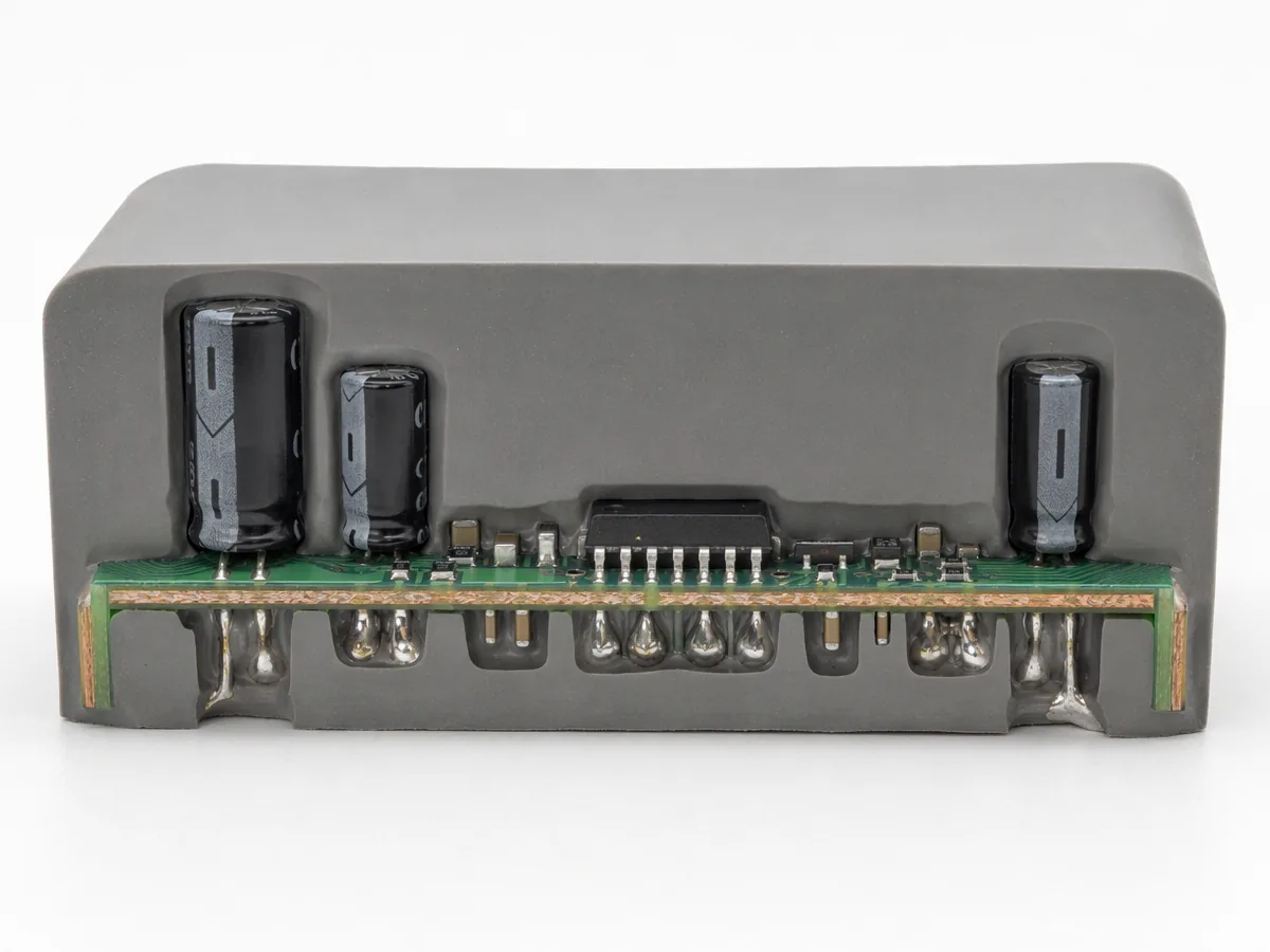 Figure 3: Section through an encapsulated board — flow around a tall component with no entrapped void above it. Achieving this is a gate-position outcome, not a machine setting.
Three consequences that change the drawing:
- Gate position is a component-relocation decision. If the tool cannot be gated to avoid a weld line across a sealed face, the connector moves on the board. That is a layout conversation to have before the board is taped out, and it is free at that point and expensive after.
- Wall thickness governs whether you can fill at all. Encapsulation walls frequently want to be 1.0–2.0 mm; under about 0.8 mm around a dense component field the flow stalls. Our wall-thickness guide explains the same physics in single-material terms.
- Flow length is not a catalogue number here. Obstacles shorten the practical flow limit far below what the resin datasheet implies. If the analysis shows a weld line where a seal is required, that is a design defect, not a moulding defect.
How Do You Prove an Overmolded Board Is Good?
Verification belongs after moulding, on 100 percent where the failure mode is electrical, and on samples where the failure mode is long-term. A board that worked before encapsulation proves nothing about the joint you just buried.
| Check | What it catches | Placement |
|---|---|---|
| Visual + dimensional | Flash, short shot, burnt tips, board warp, connector offset | Every part |
| Continuity and functional test | Opened joints, shifted parts, cracked terminations | Every part, after moulding |
| Insulation resistance / dielectric withstanding | Isolation failure across the encapsulated surface | Every part or statistical sample by risk |
| X-ray or CT | Voids under components, displaced parts, trapped solder balls | Sample per cavity and per lot initially |
| Thermal cycling | Interface fatigue, crack initiation, warp return | Qualification, then periodic |
| Sealing verification to IEC 60529 | Whether the claimed IP rating is real on this geometry | Qualification on the production tool |
| Peel / interface check where a bond is claimed | Adhesion that was assumed rather than designed | Qualification |
Electronic assembly workmanship is judged against IPC-A-610 class appropriate to your product; the moulding adds nothing to that standard but changes what you can still see. The cavity-level evidence discipline in our T1 evidence package guide applies with extra force here, because cavity-to-cavity differences show up as different weld-line positions, not just different dimensions.
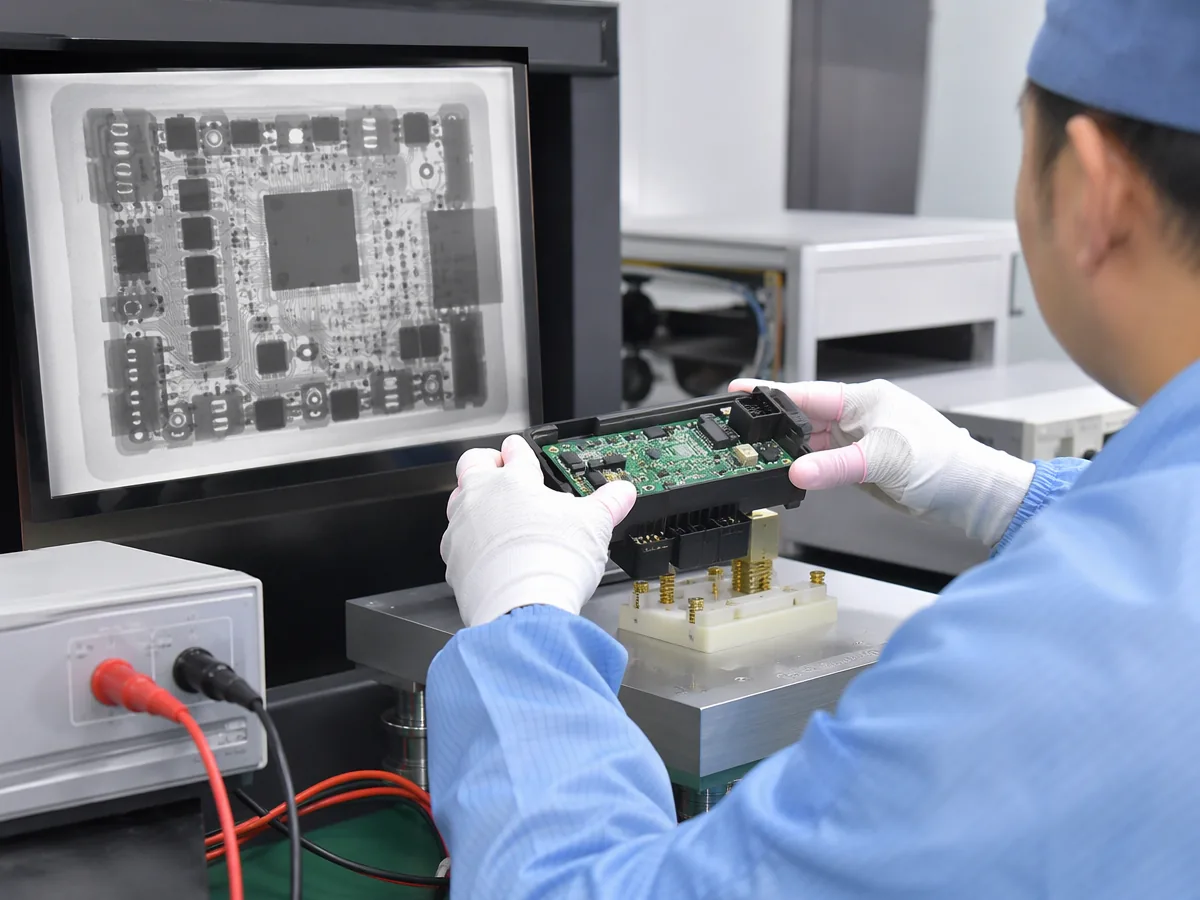 Figure 4: Post-mould electrical and imaging inspection — the only reliable look at what the tool actually did.
Write the acceptance criteria into the quality agreement before the first production order, including which of the above is 100-percent and which is sampled, and what happens to a suspect population when one fails.
The Ideal Pro Path for an Overmoulded Assembly
- Pressure audit before anything else (free, with the 24-hour quote). We run the component-force arithmetic on your actual placement and tell you which of the three processes you are in. If the answer is “potting”, you hear it from us.
- Board layout feedback. Locator features, gate-side connector placement, keep-out zones under supports, and a coplanarity requirement for the exposed interface.
- Drying and handling spec for both materials. Encapsulant dew point and dwell, plus a board floor-life rule.
- Tool with real fixturing. Support pads, connector capture, balanced fill, venting where tall parts trap air, board warp managed by support not by clamp.
- T1 in 5–10 days on straightforward tools, delivered as an evidence package with cavity identification, plus the electrical and X-ray results from Figure 4.
- Release on artefacts, then production lots shipping with dimensional and functional records per the quality agreement.
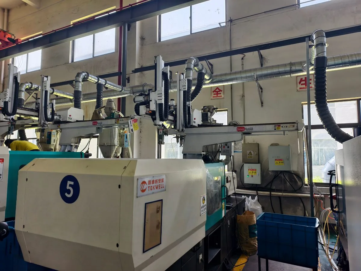 Figure 5: The press hall where the documented process that qualified your board is the one that repeats it.
When PCB Overmolding Is the Wrong Call
Sometimes. Choose potting instead when your geometry is irregular, your connectors are massive, your volumes are low, or the thermal strain on the parts must stay genuinely small. Choose a printed enclosure plus a gasket instead when you need the board accessible — an overmold is a one-way door. Choose a domestic supplier when your programme needs two-hour physical response, domestic-content sourcing, or ITAR. And do not bring an automotive safety or implant-class board to Ideal Pro, because we hold ISO 9001:2015 with RoHS and FCC documentation, not IATF 16949 or a medical device route. Buy those from certified specialists. We will still do the free DFM either way — the pressure arithmetic is useful whoever builds the tool.
요약
PCB overmolding succeeds when the process pressure is chosen against the survivable force on your weakest, tallest component — not against fill — and when the tool locates the board on hardened features instead of on parts. Pick from three genuinely different processes: conventional high-pressure overmolding for rugged layouts, low-pressure hot-melt encapsulation for populated boards, potting when geometry or thermal strain demands it. Control moisture in both resin and laminate. Gate so weld lines miss every sealed face. Then verify electrically after moulding, look inside with X-ray, cycle the qualification units thermally, and prove any IP claim to IEC 60529 on the production geometry. Send us the board file and the placement early; the free DFM answers the pressure question in a day, and at that stage it is still a layout change instead of a scrapped tool.
📞 Tel/WhatsApp: +86 156 0682 1288 · 📧 [email protected] · 🌐 Request a quote
Sources
- IEC 60529 — degrees of protection provided by enclosures (IP code): the qualification basis for any sealing claim on an overmoulded housing.
- ISO 16750 — road-vehicle environmental conditions and testing for electrical and electronic equipment: the cycling regime an automotive board must survive.
- IPC-A-610 — acceptability of electronic assemblies: the workmanship reference for the assembly entering the tool.
- ISO 9001:2015 — the documented quality framework these practices sit inside at Ideal Pro.
- Ideal Pro published shop standards: 24-hour quote with free DFM, T1 in 5–10 days on straightforward tooling, presses up to 1,600 tons, 99.8 percent on-time delivery.
- Pressure ranges here are stated as scales to verify against your machine maker and your own component layout, not as supplier guarantees.
Can you overmold a fully populated PCB with BGAs and electrolytic capacitors?
Usually not with conventional high-pressure molding. Large tall parts present the highest force and the weakest anchoring, and BGA joints are sensitive to board strain you cannot see during moulding. The realistic routes are low-pressure hot-melt encapsulation, selective potting around the problem area, or a board-layout revision that relocates the fragile parts away from the flow path. Send the placement file before you commit — this question costs nothing at layout stage and a respin after.
How do I stop the board warping during moulding?
Support the laminate on machined pads with short spans, fill symmetrically so pressure does not load one half first, and keep the melt front away from a single tall obstacle that acts as a dam. Then measure flatness on T1 parts from every cavity, not just one, because support wear and fill balance are cavity-specific. If flatness fails, the fix is usually tool support geometry and gate position — not pack pressure, which makes it worse.
Does overmolding replace conformal coating?
For moisture and splash protection it usually does a better job, because the barrier is moulded continuously around the geometry instead of brushed and masked over it. It does not replace a coating when you need the board accessible, when mass and volume are tight, or when the board will be reworked. Where you need both, verify that your encapsulant will not lift the coating — some silicone and urethane chemistries refuse to stick to specific conformal materials, and that becomes a delamination channel.
What information does a supplier genuinely need to quote this?
Three files and two answers: the board STEP or IDF plus the component placement, which faces must stay exposed and coplanar, your annual volume and target price, whether the assembly must be serviceable, and the environment it will live in. With those, a competent supplier tells you which of the three processes applies. If a quote arrives before anyone asked about component force or floor life, it was priced from the drawing’s outline.
Can a failed overmolded board be reworked or scrapped?
Effectively scrapped, and you should plan on that. Thermoplastic encapsulants can sometimes be heated and peeled, but the thermal and mechanical load on the board makes it a salvage operation rather than a repair, and thermoset potting is permanent. That is why verification sits after moulding with 100-percent electrical test, and why the reject rate — not the resin price — is usually the dominant cost in this process.
저자 소개

Alex Yu
아이디얼 프로 매뉴팩처링
알렉스는 Ideal Pro의 공동 창립자이지만, 주요 프로젝트를 총괄하거나 기술 팀을 이끌지 않을 때는 장거리 자전거 타기를 즐기거나, 동네에서 가장 맛있는 커피를 찾아다니거나, 다음 여행 계획을 세우는 모습을 볼 수 있습니다. 국제 무역 영업과 프로젝트 관리 분야에서 20년 이상의 경력을 쌓아온 그는 촉박한 마감 기한부터 까다로운 엔지니어링 문제까지, 그 사이의 모든 상황을 다 겪어보았습니다. 그는 훌륭한 성과는 충분한 휴식을 취한 마음과 맛있는 커피에서 나온다고 믿으며, 맡은 모든 프로젝트에 그와 같은 호기심과 세심한 주의를 기울입니다. 사무실에 있지 않을 때는 대개 야외 어딘가에서 새로운 장소를 탐험하며, 나중에 나눌 이야기를 수집하곤 합니다.
 English
 French
 Dutch
 German
 Japanese
 Korean