한국어



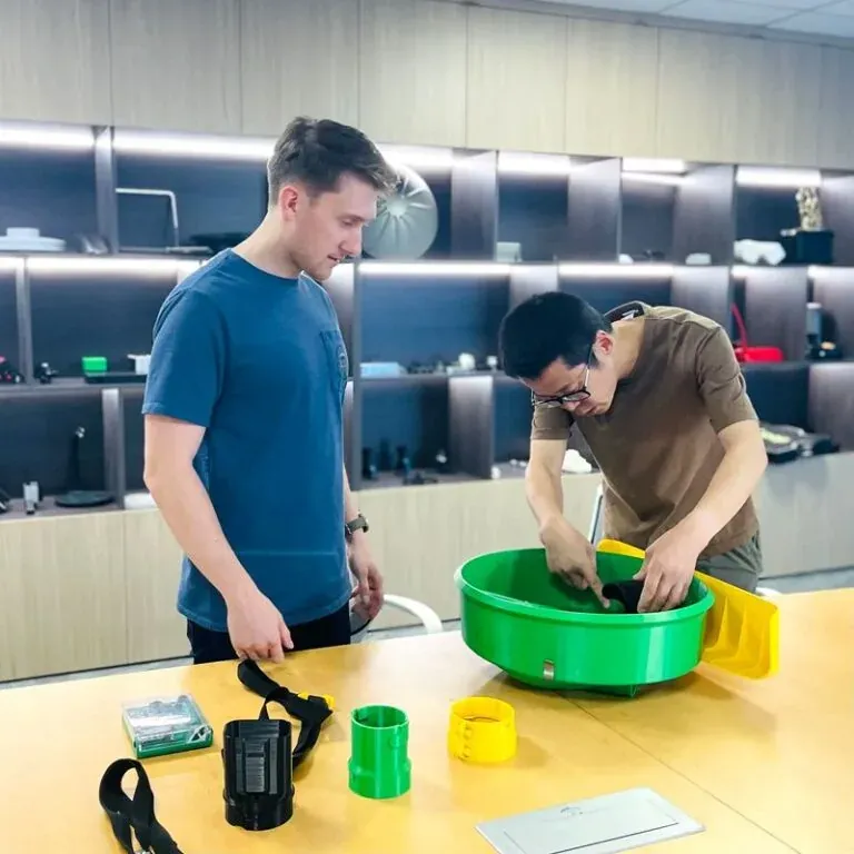
Technical Account Managers
A dedicated communication liaison provides technical support, including streamlined assistance with secure file transfers and global semiconductor supply chain compliance.
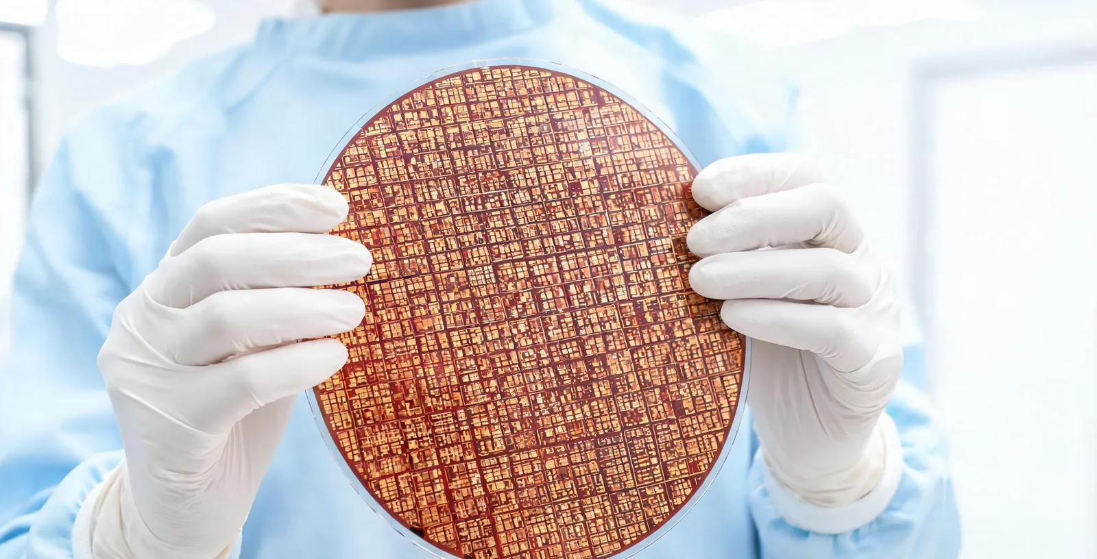
Industry / Semiconductor
Empower your silicon breakthroughs with IDEAL PRO Manufacturing. From complex wafer handling components to sub-micron lithography parts, we eliminate yield-limiting defects and accelerate your market entry through advanced CNC machining and cleanroom-ready material expertise.






ControlledCleanroom Environments
High-PurityMaterial Sourcing
Sub-MicronGeometric Tolerances
Bridge-to-MassProduction Scalability
Real-TimeSupply Chain Visibility
From sub-micron tolerances to complex thermal management, our engineering team ensures your semiconductor components meet the most stringent industry standards. We manage every critical stage including ultra-high vacuum cleaning, specialized coating, and cleanroom assembly to minimize contamination risks and ensure maximum performance for front-end or back-end processes.
Whether you require high-purity quartz components, ceramic substrates, or intricate wafer handling assemblies, our adaptive manufacturing infrastructure scales to your specific technology node. We support your project from initial R&D prototypes to high-volume production with a focus on repeatable accuracy, stable lead times, and comprehensive material traceability.
Overcome high entry costs and mitigate development risks with our flexible production model. Our no-minimum policy makes advanced semiconductor grade manufacturing accessible for early-stage testing and small-batch pilot runs. This allows you to iterate faster, optimize designs, and scale your technology without heavy upfront investment or excessive inventory overhead.
Our specialized engineering team provides rigorous Design for Manufacturability analysis specifically for semiconductor applications. By identifying potential failure points and optimizing part geometry before production begins, we significantly increase final yields, reduce expensive material waste, and accelerate your overall time-to-market in a highly competitive global landscape.


Accelerate your innovation with a manufacturing partner built for sub-micron precision, material purity, and technical reliability.
Get Your Instant Quote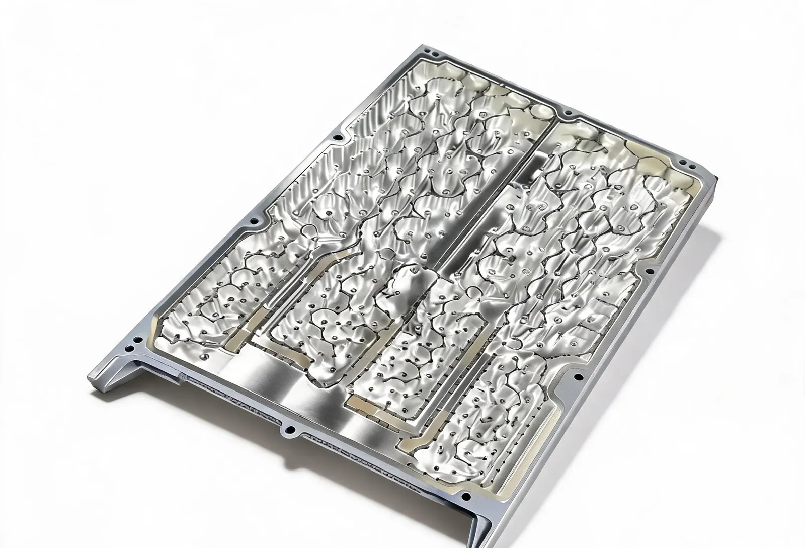
Maintaining ultra-pure environments and achieving sub-micron precision is the primary challenge in the advanced chip-making sector. At IDEAL PRO Manufacturing, we empower semiconductor equipment innovators with specialized 5-axis CNC machining and cleanroom-ready surface treatments. Our engineering team possesses the technical depth to transform complex wafer-handling designs into high-performance production hardware.
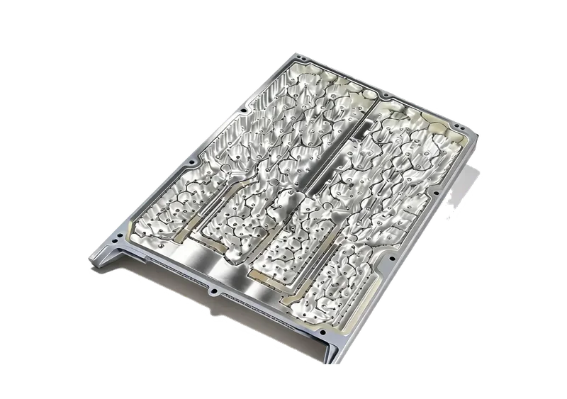
The fabrication industry demands a sophisticated range of components, from intricate gas distribution plates to large-scale vacuum chambers. Essential requirements for the semiconductor sector include:
Below are some of the specialized parts we manufacture for global leaders in the semiconductor sector:
Explore how we solve complex fabrication challenges to deliver high-yield semiconductor hardware with precision expertise.

The client, a leading lithography equipment innovator, sought to eliminate micro-particle contamination within critical processing environments. IDEAL PRO Manufacturing utilized advanced 5-axis CNC machining to fabricate complex internal chamber geometries that enhanced gas flow dynamics while maintaining strict vacuum seal integrity. Our precise DFM insights minimized material porosity and ensured zero outgassing in ultra-high vacuum production lines.
250+
Custom Chambers Delivered
35%
Thermal Stabilization Gain
0.01mm
Dimensional Tolerance Held
45%
Outgassing Rate Reduction
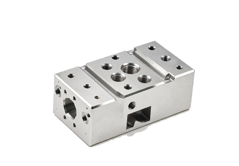
A wafer-fab equipment maker needed a compact gas-delivery manifold with mirror-smooth internal bores to prevent particle entrapment. IDEAL PRO machined the housing from forged 316L stainless steel using 5-axis turning and milling, then electropolished every flow path. The multi-port body holds tight concentricity and leak-free sealing across dozens of connection points.
Ra 0.2
Electropolished Bore Finish
0.005mm
Bore Concentricity
0
Helium-Leak Failures
316L
High-Purity Stainless

For an equipment front-end module (EFEM) used in 300mm wafer handling, IDEAL PRO produced hard-anodized aluminum structural rails with permanent laser-engraved alignment indices. The rails deliver wear-free guidance for robot end-effectors while the chemical-resistant anodized layer survives cleanroom wipe-down chemistries without corrosion or particulate shedding.
±0.02mm
Rail Straightness
500HV
Hard-Anodized Layer
Cleanroom-Ready
Class 5 Cleanroom Build
100%
Laser-Mark Traceability
Our team of precision manufacturing experts operates strategically behind the scenes to streamline your fabrication orders. We manage the entire lifecycle to guarantee immaculate contamination control and keep your engineers fully aligned throughout the process.
A dedicated communication liaison provides technical support, including streamlined assistance with secure file transfers and global semiconductor supply chain compliance.

Expert DFM solutions and yield-maximization strategies tailored by in-house specialists to optimize your advanced wafer handling and vacuum component designs.
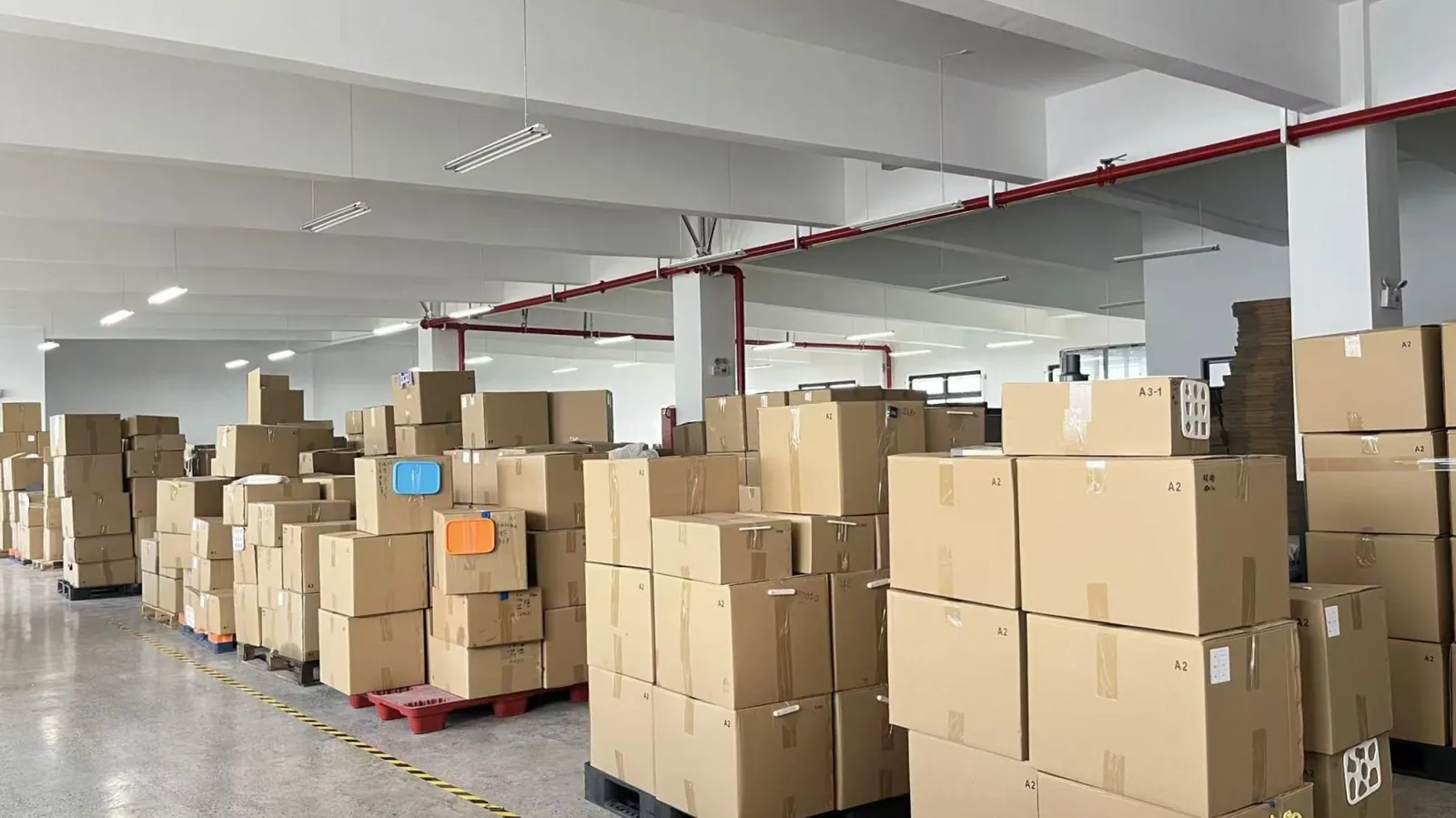
Seamless cleanroom packaging fulfillment and shipping efficiency optimization managed by experienced clean-chain logistics experts to prevent transport contamination.
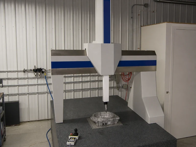
Our skilled inspection teams utilize advanced CMM and non-destructive testing to ensure your precision parts meet exact micro-scale geometric specifications.
IDEAL PRO Manufacturing offers a comprehensive suite of advanced manufacturing processes tailored for high-yield semiconductor components and critical sub-assemblies.
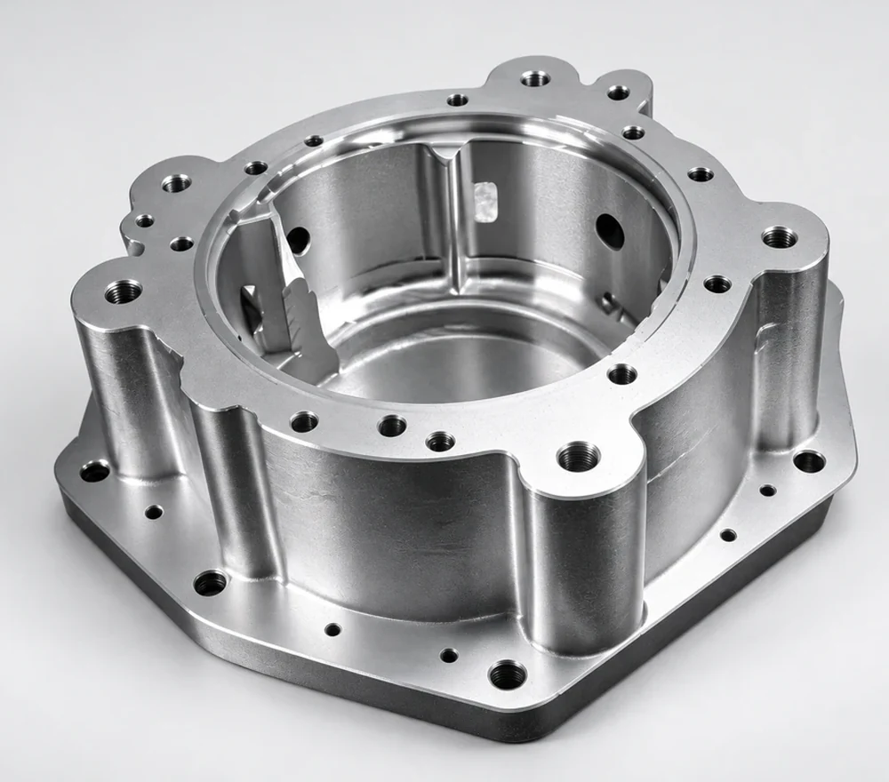
Sub-micron milling and turning for high-purity applications. Achieve strict micrometer tolerances, zero-burr finishes, and rapid turnarounds for your complex wafer handling environment.
자세히 알아보기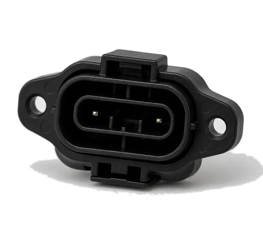
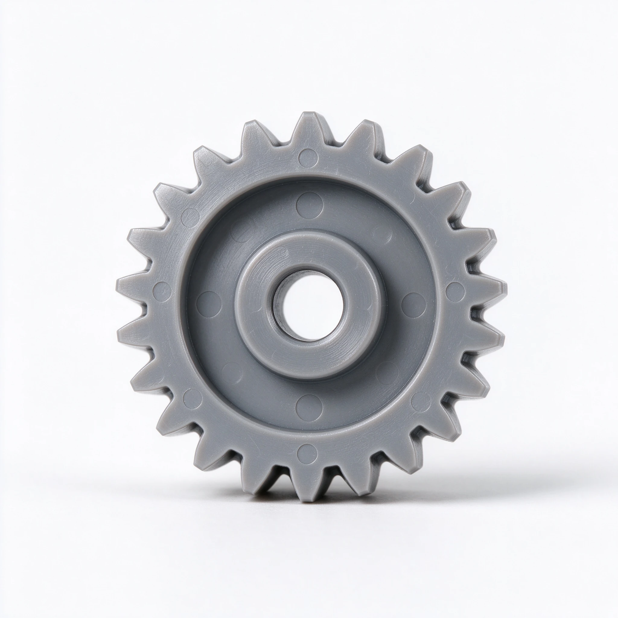
Ultra-pure engineering plastics molding from micro-scale prototypes to scalable production volume. Eliminate contamination risks with ESD-safe materials tailored for technology nodes.
자세히 알아보기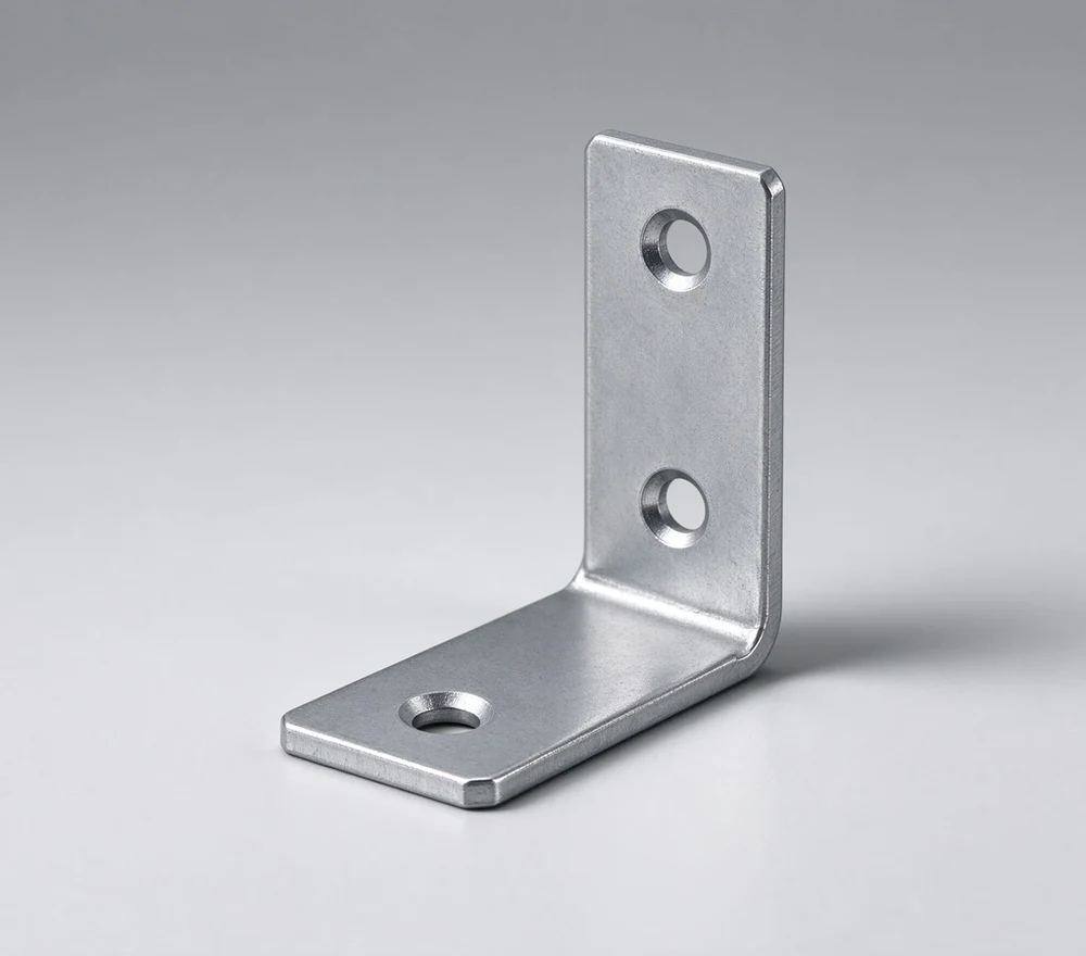
Expert laser cutting, specialized forming, and orbital welding. Gain cleanroom-ready enclosures and vacuum-tight frames with full material traceability in 3 days.
자세히 알아보기
High-density additive manufacturing for functional testing components and specialized jigs. Accelerate iteration cycles with geometric freedom and rapid 24-hour delivery.
자세히 알아보기Over the decades we have developed deep technical expertise that allows IDEAL PRO Manufacturing to master complex fabrication projects. Explore our gallery of precision-engineered semiconductor prototypes and ultra-high-purity production components for our global network partners.


All semiconductor components shown are proprietary IDEAL PRO Manufacturing designs, authorized for public display.
We offer an elite range of advanced material possibilities with all our manufacturing processes. Some premium choices for high-yield semiconductor fabrication projects are structured below.
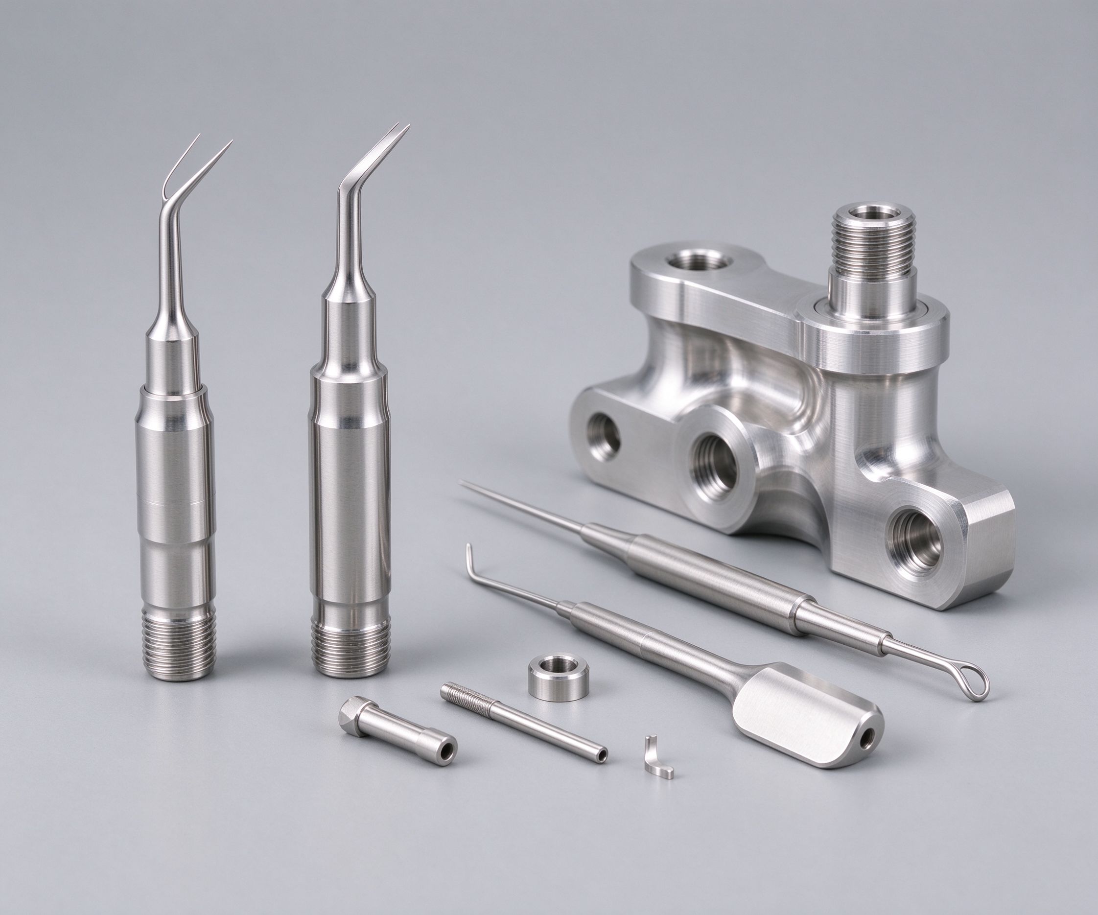
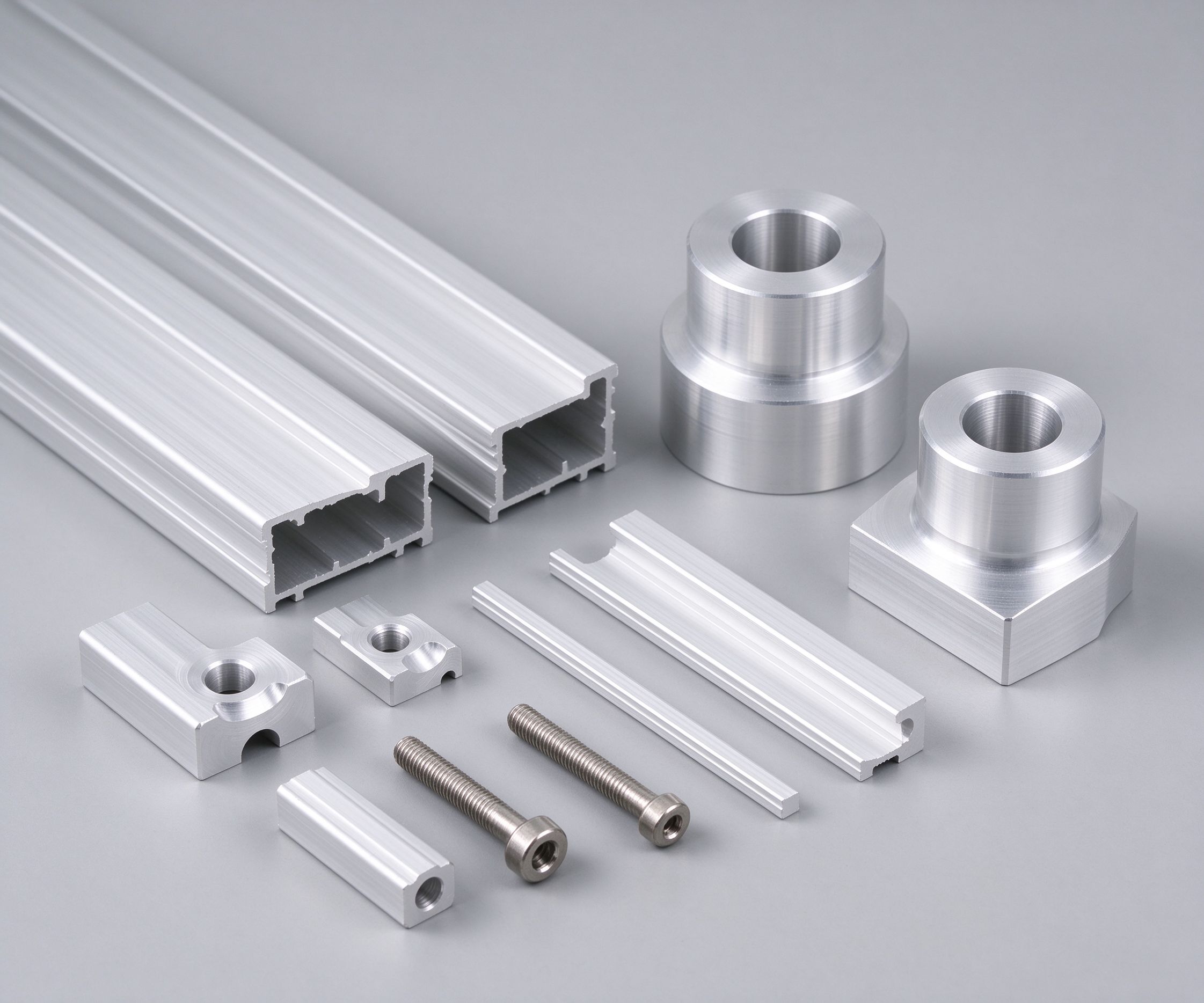
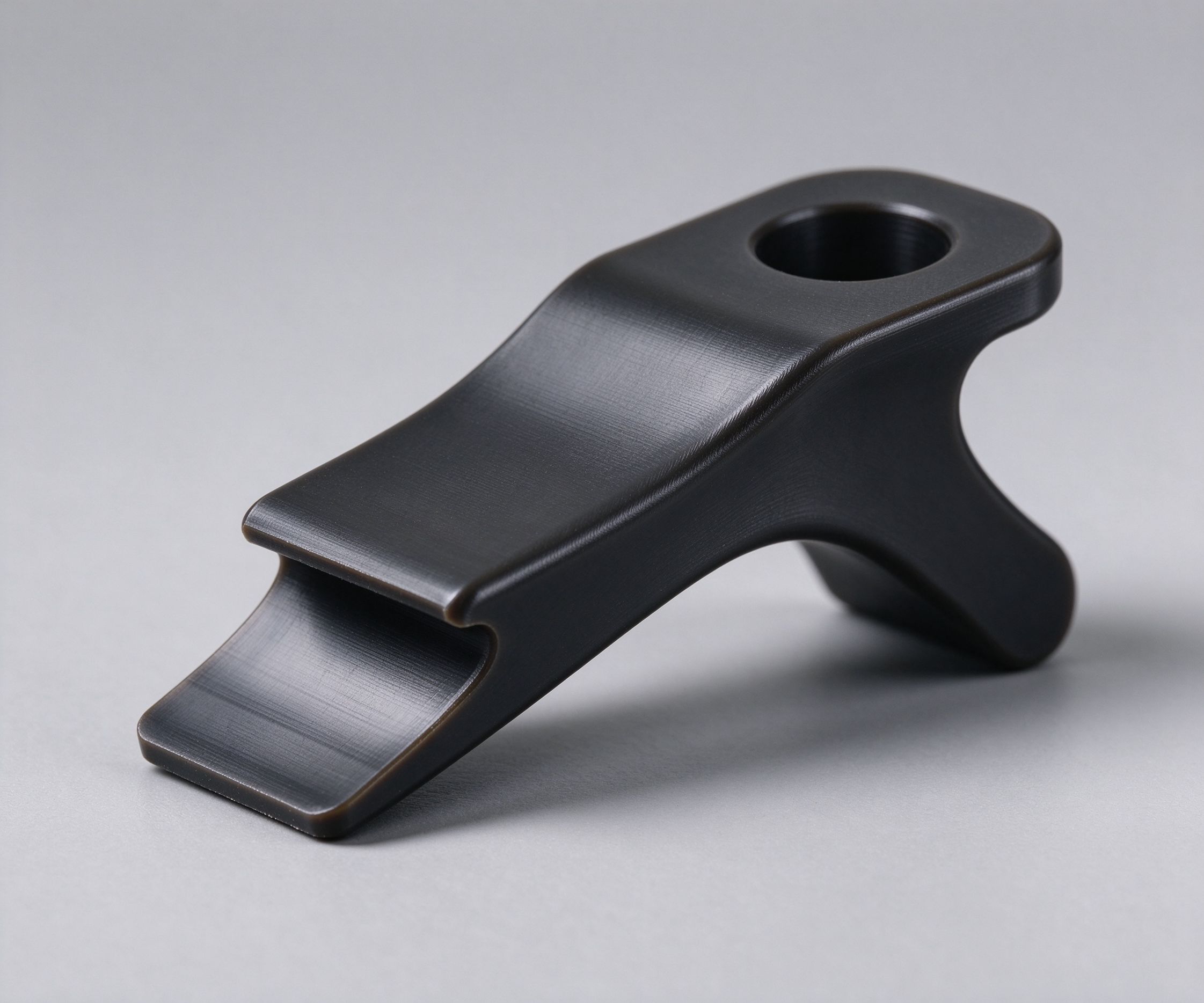
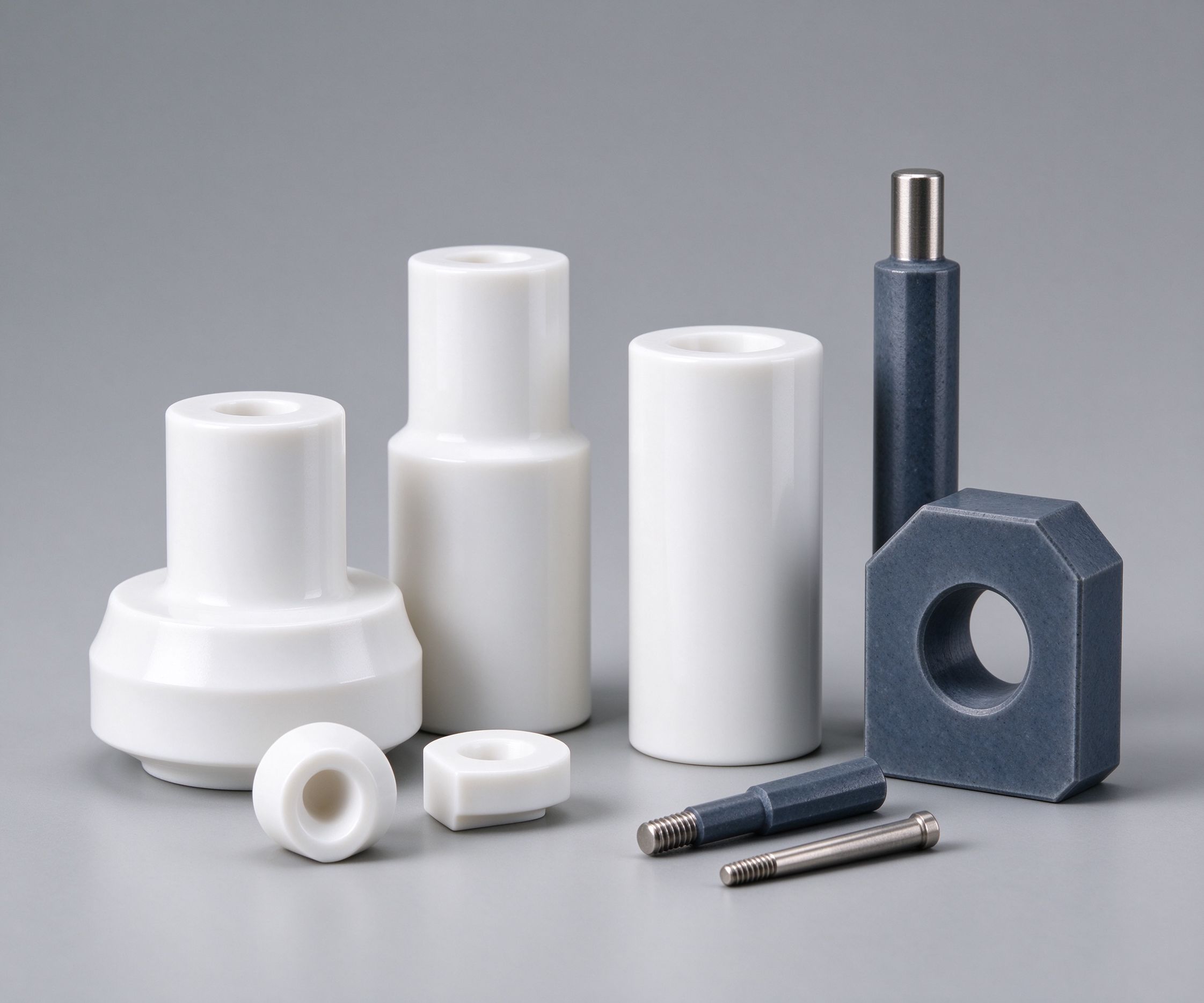
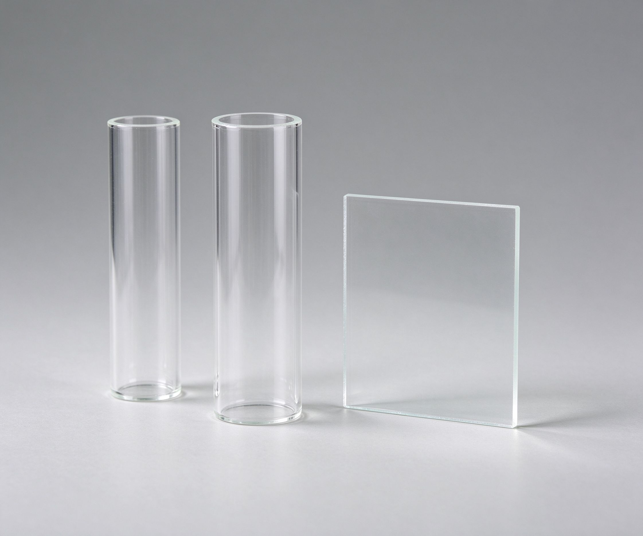
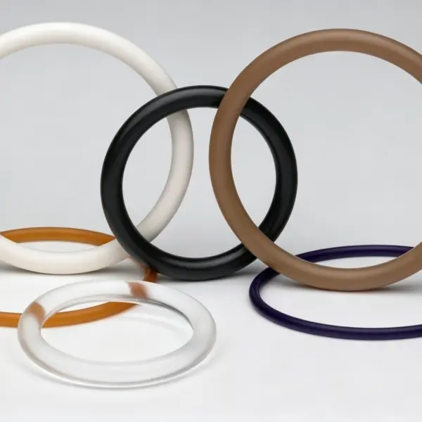

Partner with IDEAL PRO Manufacturing for ultra-precision semiconductor components. Get expert material guidance and an instant quote for your next fabrication project.
IDEAL PRO Manufacturing offers wide variety high level surface finishes for high-yield chips fabrication. We only list some of the common finishing options for custom precision components in semiconductor industry.



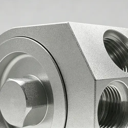

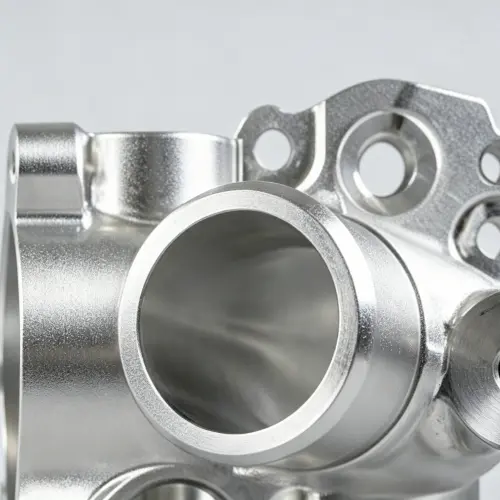
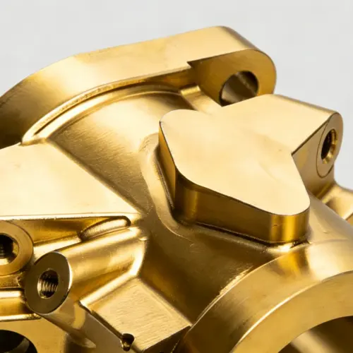
We have engineering capabilities within our advanced processes ideal for semiconductor equipment manufacturing. A few common system applications include:
Learn a number of ways to optimize your CNC machining parameters to achieve sub-micron tolerances, eradicate surface microscopic defects, and lower manufacturing costs.
Read Design TipLearn about the specialized material properties of ESD-safe polymers and the precise molding processes used to eliminate outgassing risks in high-tech fabrication.
Read Guide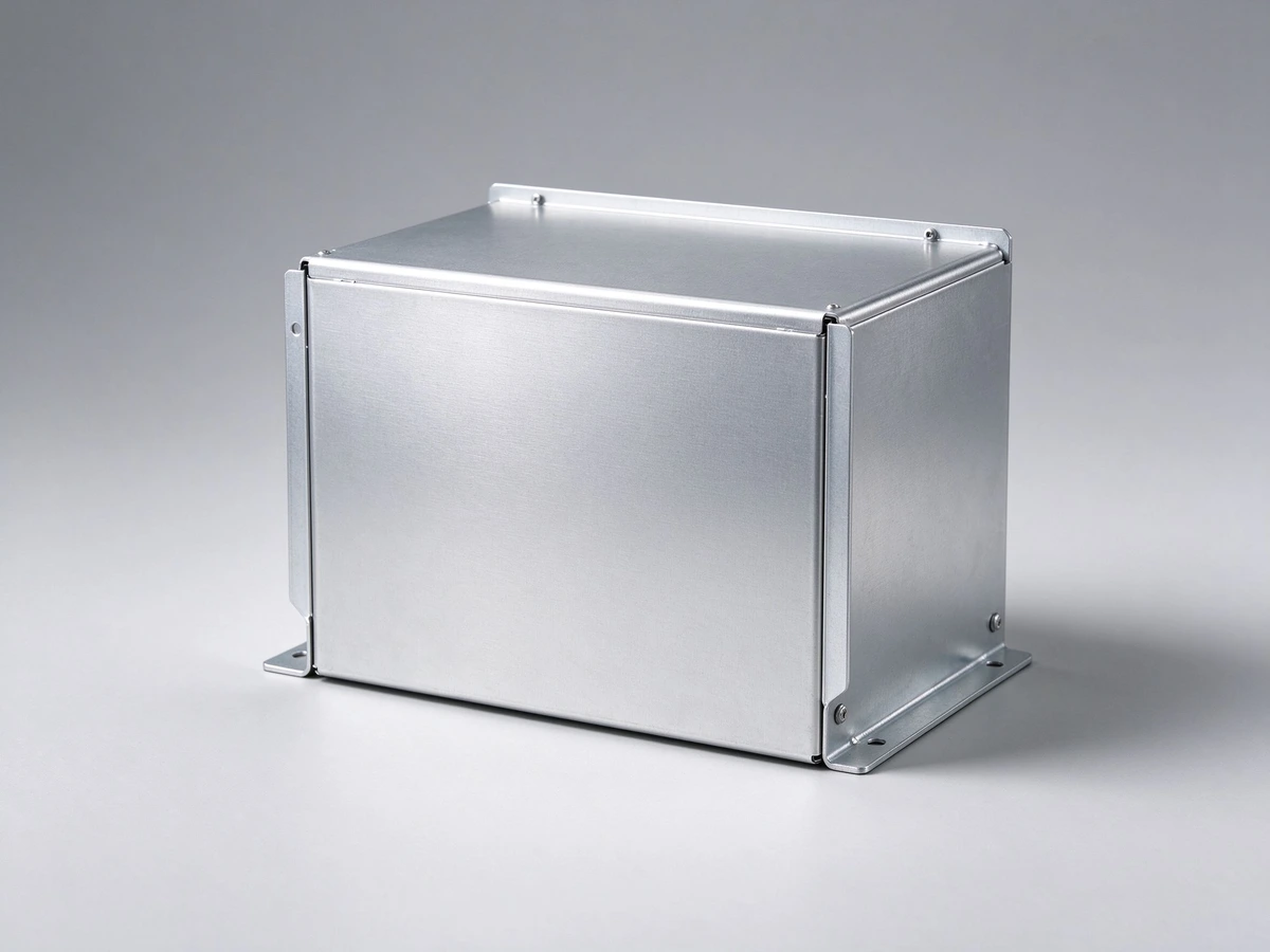
Discover expert methods to modify your sheet metal geometries for cleanroom enclosures, securing perfect vacuum-tight orbital welds while protecting delicate system electronics.
Watch Webinar
Additive manufacturing is an ideal way to produce intricate, unmachinable internal channels or customized assembly fixtures with zero tooling lead times.
Read Case StudyIDEAL PRO Manufacturing의 최신 소식과 공지 사항을 놓치지 마세요. 아래에서 최신 기사를 확인해 보세요.
 English English
 French
 Dutch
 German
 Japanese
 Korean